


A chip package is simply a substrate that carries the integrated circuit (die) produced by Foundry, with the pins pinned out, and then fixed and packaged as a whole. It protects the chip and is the equivalent of a shell for the chip, not only securing and sealing it, but also enhancing its electrical and thermal properties. Therefore, packaging is very important for CPUs and other LSI integrated circuits.
The types of packages can be roughly divided into two types: DIP double in-line packages and SMD chip packages.
In terms of structure, the package has evolved from the earliest transistor TO (e.g. TO-89, TO92) package to the double inline package, followed by the SOP small form factor package developed by PHILIP, and then gradually derived from SOJ (J-type pin small form factor package), TSOP (thin small form factor package), VSOP (very small form factor package), SSOP (reduced SOP) , TSSOP (thin reduced SOP) and SOT (small form factor transistor), SOIC (small form factor integrated circuit), etc.
In terms of material media, these include metals, ceramics, plastics, plastics, and many circuits that require high intensity operating conditions such as military and aerospace grade still have a large number of metal packages.
The following is a list of the 40 most common types of packages:
In terms of structure, the package has evolved from the earliest transistor TO (e.g. TO-89, TO92) package to the double inline package, followed by the SOP small form factor package developed by PHILIP, and then gradually derived from SOJ (J-type pin small form factor package), TSOP (thin small form factor package), VSOP (very small form factor package), SSOP (reduced SOP) , TSSOP (thin reduced SOP) and SOT (small form factor transistor), SOIC (small form factor integrated circuit), etc.
In terms of material media, these include metals, ceramics, plastics, plastics, and many circuits that require high intensity operating conditions such as military and aerospace grade still have a large number of metal packages.
1.BGA package (ball grid array)
Ball contact display, one of the surface mount packages. A spherical bump is created on the back of the printed substrate in place of the pins, and the LSI chip is assembled on the front of the printed substrate and then sealed with a moulded resin or potting method. Also known as a bump display carrier (PAC).
This is a type of package used for multi-pin LSIs, which can have more than 200 pins. The package body can also be made smaller than a QFP (Quadruple Side Pin Flat Package). For example, a 360-pin BGA with 1.5 mm pin centres is only 31 mm square, while a 304-pin QFP with 0.5 mm pin centres is 40 mm square. The BGA does not have to worry about pin deformation like the QFP.
The package was developed by Motorola in the USA and was first adopted in devices such as portable telephones and is likely to become common in the USA for personal computers in the future. Initially, BGAs had a pin (bump) centre distance of 1.5 mm and a pin count of 225. 500-pin BGAs are now also being developed by some LSI manufacturers.
The problem with BGAs is the cosmetic inspection after reflow. It is not clear whether this is a valid method of inspection. It is thought that due to the large centre distance of the solder, the connection can be regarded as stable and can only be dealt with by functional inspection. Motorola USA refers to packages sealed with moulded resin as OMPAC and those sealed by potting as GPAC (see OMPAC and GPAC).
2. BQFP package (quad flat packagewith bumper)
A quad flat packagewith bumper is a package in which the four corners of the packagewith bumper prevent the pins from bending and deforming during transport. This package is mainly used by US semiconductor manufacturers in circuits such as microprocessors and ASICs. The pin centres are 0.635 mm apart and the number of pins ranges from 84 to around 196 (see QFP).
3. Butt joint pin grid array (PGA)
An alternative name for surface mount PGAs (see surface mount PGA).
4.C-(ceramic) package
A notation indicating a ceramic package. For example, CDIP indicates a ceramic DIP, a notation that is often used in practice.

5.Cerdip package
Ceramic double in-line package sealed with glass for ECL RAM, DSP (Digital Signal Processor) and other circuits. Cerdip with glass window
Used for UV-erasable EPROMs and microcomputer circuits with internal EPROMs, etc. The pin centres are 2.54 mm apart and the number of pins ranges from 8 to 42. In Japan, this package is known as DIP-G (G for glass sealed).
6.Cerquad package
One of the surface mount packages, the ceramic QFP with underseal, is used to package logic LSI circuits such as DSPs. Cerquad with a window is used to package EPROM circuits. It has better thermal dissipation than the plastic QFP and can accommodate 1.5 to 2W of power under natural air cooling conditions. However, the cost of the package is 3 to 5 times higher than the plastic QFP. Pin centres are available in 1.27mm, 0.8mm, 0.65mm, 0.5mm, 0.4mm and other specifications. The number of pins ranges from 32 to 368.
Ceramic chip carriers with pins, one of the surface-mount packages, have pins leading from the four sides of the package in a zigzag shape. The windowed version is used to package UV erasable EPROMs and microcomputer circuits with EPROMs, etc. This package is also known as QFJ, QFJ-G (see QFJ).
7.CLCC package (ceramic leadedchip carrier)
Ceramic leaded chip carrier with pins, one of the surface mount packages, with pins leading out from the four sides of the package in a dingus shape. The windowed version is used to package UV erasable EPROMs and microcomputer circuits with EPROMs, etc. This package is also known as QFJ, QFJ-G (see QFJ).
8. COB package (chip on board)
Chip on board packaging, is one of the bare chip mounting technology, the semiconductor chip is mounted on the printed circuit board, the electrical connection between the chip and the substrate is realized by the lead stitching method, the electrical connection between the chip and the substrate is realized by the lead stitching method, and it is covered with resin to ensure the *. Although COB is the simplest bare chip mounting technology, it is not as densely packed as TAB and flip chip soldering.
9. DFP (dual flat package)
Double side pin flat package. It is an alternative name for SOP (see SOP). It used to be called this, but is now largely unused.


10. DIC (dual in-line ceramic package)
Alias for ceramic DIP (with glass seal) (see DIP).
11. DIL (dual in-line)
Alias for DIP (see DIP). This name is mostly used by European semiconductor manufacturers.
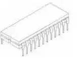
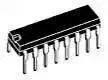
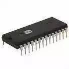
12. DIP (dual in-line package) Double in-line package
One of the cartridge packages, the pins are led from both sides of the package, the package material has two kinds of plastic and ceramic. DIP is the most popular cartridge package, the application range includes standard logic IC, memory LSI, microcomputer circuits, etc.
The pin centres are 2.54mm apart and the number of pins ranges from 6 to 64. The package width is usually 15.2mm and some packages with a width of 7.52mm and 10.16mm are called skinny DIP and slim DIP respectively. Also, ceramic DIPs sealed with low melting point glass are called cerdip (see cerdip).
13. DSO (dual small out-lint)
An alias for SOP (see SOP). Some semiconductor manufacturers use this name.
14. DICP (dual tape carrier package)
One of the TCP (dual tape carrier packages). The pins are made on an insulating tape and lead out from both sides of the package. Due to the use of TAB (automatic tape carrier soldering) technology, the package profile is very thin. Commonly used for LCD driver LSIs, but most are customised. In addition, a 0.5mm thick memory LSI booklet package is in the development stage. In Japan, the DICP is named DTP according to the EIAJ (Electronic Industries and Machinery Association of Japan) standard.
15. DIP (dual tape carrier package)
As above. Naming of the DTCP in the JEMIC standard (see DTCP).
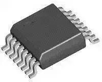
16. FP (flat package)
Flat package. An alternative name for QFP or SOP (see QFP and SOP), one of the surface mount packages. Some semiconductor manufacturers use this name.

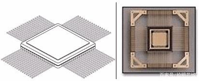
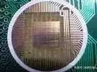
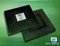
17. Flip-chip
Flip-chip. One of the bare-chip packaging technologies, in which a metal bump is made in the electrode area of the LSI chip and then the metal bump is pressure-soldered to the electrode area on the printed substrate. The area occupied by the package is essentially the same as the size of the chip. It is the smallest and thinnest of all packaging technologies.
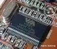
However, if the coefficient of thermal expansion of the substrate is different from that of the LSI chip, a reaction can occur at the joint, which can affect the reliability of the connection. The LSI chip must therefore be reinforced with resin and a substrate material with essentially the same coefficient of thermal expansion must be used. The SiS 756 Northbridge chip is available in the latest Flip-chip package and fully supports AMD Athlon 64/FX central processors.
It supports PCI Express X16 interface, providing up to 8GB/s bi-directional transfer bandwidth for graphics cards. Supports the highest HyperTransport Technology with up to 2000MT/s MHz transfer bandwidth. Built-in SiS exclusive AdvancedHyperStreaming Technology, MuTIOL 1G Technology.
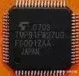
18. FQFP (fine pitch quad flat package)
Small pin-centre pitch QFPs, usually with a pin-centre distance of less than 0.65 mm (see QFP). Some conductor manufacturers use this name. Plastic Quad Flat Package (PQFP) The PQFP package is the most common form of package.
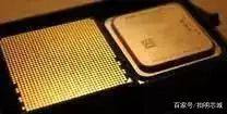
This is the most common form of package, with very small distances between the pins and very thin pins, and is used for many large-scale or very large integrated circuits, usually with more than 100 pins. 80286, 80386 and some 486 motherboard chips in the Intel family of CPUs use this form of package. Chips in this type of package must be soldered to the board using SMT technology (surface mount equipment).
Chips mounted using SMT technology do not require holes to be punched in the board, but generally have designed solder joints on the surface of the board for the corresponding pins. The chips are soldered to the motherboard by aligning the pins with the corresponding solder joints. SMT technology has also been used extensively in the soldering of chips, and since then many advanced packaging technologies have required SMT soldering.
The following is a 286 processor chip in AMD's QFP package. 0.5mm solder area centre distance, 208 I/O pins, form factor 28 x 28mm, chip size 10 x 10mm, then chip area / package area = 10 x 10 / 28 x 28 = 1:7.8, which shows that the package size of QFP has been greatly reduced compared to DIP.
19. CPAC (globetop pad array carrier)
Motorola's alias for BGA (see BGA).
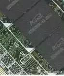
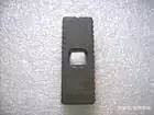
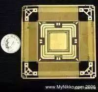
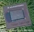
20. CQFP Military Chip CeramicQuad Flat-pack Package
The chip below is a military chip package (CQFP), which is what the package looks like before it is put into a crystal. This type of package is only found in military and aerospace industry wafers. There is a thick gold barrier (raised, not visible in the photo) next to the chip slot to protect it from radiation and other interference.
On the outside there are screw holes to hold the chip firmly in place on the main board. The most interesting feature is the gold plated pins around the periphery, which greatly reduce the thickness of the chip package and provide excellent heat dissipation.
21. PLCC packaging
PLCC is a plastic chip package carrier with leads. The PLCC package is suitable for SMT surface mount technology for PCB mounting and wiring and has the advantages of small form factor and high reliability.
PLCC is a special pin chip package, which is a kind of SMD package, the pins of this package are bent inwards at the bottom of the chip, so the pins of the chip are not visible in the top view of the chip. This type of chip is soldered using a reflow process, which requires special soldering equipment, and it is also very troublesome to remove the chip during debugging, so it is rarely used nowadays.
ZLG has been specialising in the chip burning industry for over ten years and its programmers support and provide burn-in holders for various package types of ICs for mass production in factories.


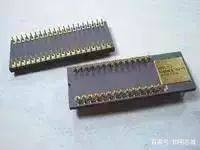
22. Pin Grid Array (Surface Mount Type)
The surface mount type PGA is usually a cartridge type package with a pin length of about 3.4 mm. surface mount type PGA has a display of pins on the bottom side of the package with a length from 1.5 mm to 2.0 mm. the mounting is done by bump-soldering with the printed substrate, so it is also called bump-soldering PGA.
Because the pin centre distance is only 1.27mm, half the size of a cartridge type PGA, the package body can be made smaller, while the number of pins is higher than that of a cartridge type (250 to 528), making it a package for large-scale logic LSI. The package substrates are multilayer ceramic substrates and glass epoxy printed substrates. The use of multilayer ceramic substrates for packages is already practical.
23. JLCC package (J-leaded chip carrier)
J-shaped pin chip carrier. Alias for CLCC with window and ceramic QFJ with window (see CLCC and QFJ). The name used by some semiconductor manufacturers.
24. LCC package (Leadless chip carrier)
Leadless chip carrier. A surface mount package in which only the four sides of the ceramic substrate are in contact with the electrodes and no pins. It is a package for high-speed and high-frequency ICs, also known as a ceramic QFN or QFN-C (see QFN).
25. LGA package (land grid array)
Contact display package. This is a package with an array of land grid contacts on the bottom side. When assembled, it can be inserted into the socket. Ceramic LGAs with 227 contacts (1.27mm centre distance) and 447 contacts (2.54mm centre distance) are now in use for high-speed logic LSI circuits.
LGAs are able to accommodate more input and output pins in a smaller package than QFPs. In addition, due to the low impedance of the leads, they are suitable for high-speed LSI. However, due to the complexity and high cost of making sockets, they are not largely used now. Demand for them is expected to increase in the future.

26. Lead-on-Chip (LSI) packaging
One of the LSI packaging technologies, the front of the leadframe is positioned above the chip and a bumpy solder joint is made near the centre of the chip, which is electrically connected by a lead stitch. Compared to the original structure where the leadframe is placed near the side of the chip, the chip can be accommodated in the same size package up to a width of about 1mm.
27 .LQFP package (low profile quadflat package)
A QFP with a package body thickness of 1.4mm, this is the name used by the Japan Electronics Machinery Industry Association for the new QFP form factor.
28 .L-QUAD package
One of the ceramic QFPs. The package substrate is made of aluminium nitride, and the thermal conductivity of the base is 7 to 8 times higher than that of aluminium oxide, providing better heat dissipation. The frame of the package is made of aluminium oxide and the chip is sealed by potting method, thus suppressing the cost. It is a package developed for logic LSIs and can accommodate W3 power under natural air cooling conditions.
The 208-pin (0.5mm centre pitch) and 160-pin (0.65mm centre pitch) packages for LSI logic have been developed and have been in series production since October 1993.
29. MCM packages
Multi-chip assemblies. A package in which multiple bare semiconductor chips are assembled on a wiring substrate.
Depending on the substrate material, there are three main categories: MCM-L, MCM-C and MCM-D.
MCM-L is a component that uses the usual glass epoxy resin multilayer printed substrate. The wiring density is not very high and the cost is low.
MCM-C is a component that uses thick film technology to form multilayer wiring with ceramic (alumina or glass-ceramic) as the substrate, similar to thick film hybrid ICs that use multilayer ceramic substrates. There are no significant differences between the two. The wiring density is higher than that of the MCM-L.
The MCM-D is a multilayer wiring assembly using thin film technology with ceramic (alumina or aluminium nitride) or Si or Al substrates. The wiring density is the highest of the three components, but the cost is also high.
30. MFP package (mini flatpackage)
A small, flat package. Alias for plastic SOP or SSOP (see SOP and SSOP). The name used by some semiconductor manufacturers.
31. MQFP (metric quad flatpackage)
A classification of QFPs according to the JEDEC (Joint Electronic Devices Committee) standard. It refers to a standard QFP with a pin centre distance of 0.65 mm and a body thickness of 3.8 mm to 2.0 mm (see QFP).
32. MQUAD package (metal quad)
A QFP package developed by Olin, USA. The base plate and cover are made of aluminium and sealed with adhesive. It allows 2.5W to 2.8W of power under natural air-cooled conditions. Production started in 1993 with a licence from Nihon Kohki Kogyo.
33. MSP package (mini squarepackage)
The QFI is the name given by the Japan Electronics Machinery Industry Association.
34. OPMAC package (over moulded padarray carrier)
Molded resin sealed bump display carrier. The name used by Motorola in the USA for moulded resin sealed BGAs (see BGA).
35. P-(plastic) Packaging
A notation indicating a plastic package. For example, PDIP means plastic DIP.
36. PAC package (pad arraycarrier)
Bump display carrier, alias of BGA (see BGA).

37. PCLP (printed circuit board leadless package)
Printed circuit board leadless package. The name used by Fujitsu Japan for plastic QFN (plastic LCC) (see QFN). Pin centres are available in 0.55mm and 0.4mm sizes. Currently in the development phase.
38. PFPF (plastic flat package)
Plastic flat package. Alias for plastic QFP (see QFP). The name used by some LSI manufacturers.
39. PGA (pin grid array)
Pin array package. One of the cartridge-type packages in which the vertical pins on the bottom side are arranged in a display pattern. The base material is basically a multilayer ceramic substrate. Where the material is not specifically named, it is mostly ceramic PGAs, used for high-speed, large-scale logic LSI circuits. The cost is high. The pin centres are usually 2.54 mm apart and the number of pins ranges from 64 to around 447.
To reduce costs, the package substrate can be replaced by a glass epoxy printed substrate. There are also plastic PGAs with 64 to 256 pins, and a short surface mount PGA with 1.27mm pin centres (touch-solder PGA). (See surface mount PGA).
40. Piggy Back
A packaged package. A ceramic package with a socket, similar in shape to DIP, QFP, QFN. Used in the development of devices with microcomputers to evaluate program verification operations. For example, the EPROM is inserted into the socket for debugging. These packages are largely bespoke and are not widely available on the market.
In Stock
Please send RFQ , we will respond immediately.
- English
- French
- German
- Portuguese
- Spanish
- Russian
- Japanese
- Korean
- Arabic
- Irish
- Greek
- Turkish
- Italian
- Danish
- Romanian
- Indonesian
- Czech
- Afrikaans
- Swedish
- Polish
- Basque
- Catalan
- Esperanto
- Hindi
- Lao
- Albanian
- Amharic
- Armenian
- Azerbaijani
- Belarusian
- Bengali
- Bosnian
- Bulgarian
- Cebuano
- Chichewa
- Corsican
- Croatian
- Dutch
- Estonian
- Filipino
- Finnish
- Frisian
- Galician
- Georgian
- Gujarati
- Haitian
- Hausa
- Hawaiian
- Hebrew
- Hmong
- Hungarian
- Icelandic
- Igbo
- Javanese
- Kannada
- Kazakh
- Khmer
- Kurdish
- Kyrgyz
- Latin
- Latvian
- Lithuanian
- Luxembou..
- Macedonian
- Malagasy
- Malay
- Malayalam
- Maltese
- Maori
- Marathi
- Mongolian
- Burmese
- Nepali
- Norwegian
- Pashto
- Persian
- Punjabi
- Serbian
- Sesotho
- Sinhala
- Slovak
- Slovenian
- Somali
- Samoan
- Scots Gaelic
- Shona
- Sindhi
- Sundanese
- Swahili
- Tajik
- Tamil
- Telugu
- Thai
- Ukrainian
- Urdu
- Uzbek
- Vietnamese
- Welsh
- Xhosa
- Yiddish
- Yoruba
- Zulu
- Kinyarwanda
- Tatar
- Oriya
- Turkmen
- Uyghur